
What are the process requirements for single layer flexible PCBs?
Flexible circuit boards can be divided into two types based on the combination of substrate and copper foil: adhesive flexible board and non adhesive flexible board. Among them, the flexibility of non adhesive flexible circuit boards, the bonding force between copper foil and substrate, and the flatness of solder pads are better than those with adhesive. Therefore, non adhesive flexible circuit boards are more expensive than adhesive flexible circuit boards in terms of price.
"We know that flexible PCBs can be bent, and are usually used in situations where bending is required. If the design or process is not reasonable, defects such as microcracks and open welds can easily occur.". Today, the editor of Jieduobang PCB will discuss with you the relevant knowledge of flexible circuit board process requirements. Considering the price issue, most flexible PCBs on the market currently use adhesive based flexible PCBs.
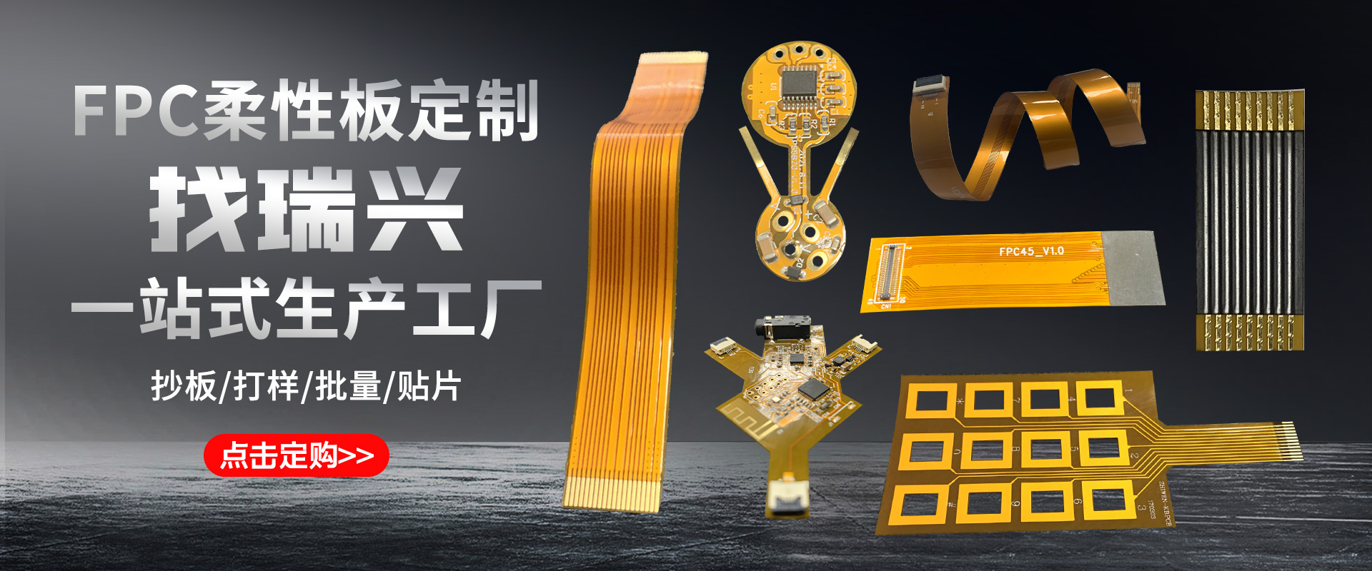
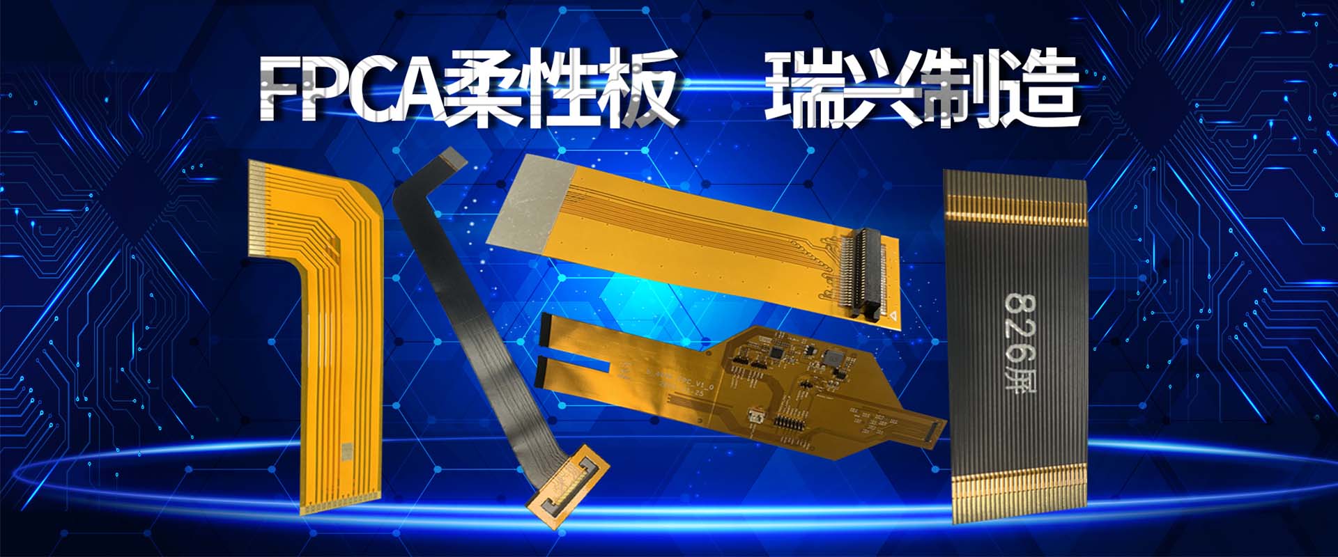
According to the number of layers of conductive copper foil, flexible Pcbs can be divided into single layer boards, double layer boards, multi-layer boards, and double-sided boards. Taking single layer flexible PCBs as an example, we will explain the process requirements for flexible circuit boards.
After cleaning, use the rolling method to combine the two. Then, the exposed solder pad is electroplated with gold or tin for protection. In this way, the board is ready. Generally, small circuit boards are also stamped into corresponding shapes.
Single-layer flexible PCBs are the simplest flexible circuit boards. The raw materials are purchased in two types: substrate+transparent adhesive+copper foil and protective film+transparent adhesive. Wait for the required circuit through processing such as etching the copper foil; The protective film shall be drilled to expose the corresponding pad. After cleaning the two, use the rolling method to combine the two, and then use electroplated gold or tin to protect the exposed solder pads. This is how the large plate is made. Generally, small circuit boards are also stamped into corresponding shapes.
Of course, there are also cases where the solder resist layer is printed directly on the copper foil without the need for a protective film. The mechanical strength of the circuit board produced by this method will deteriorate, but the production cost is relatively lower. This method is generally used in situations where the strength requirements are not high and the price requirements are low. However, the editor still recommends that you use the method of applying protective film.
-
 Hotline: 0755-27059800
Miss Guan: 13530507787 mailbox: szrxfpc@163.com address: Baoan District, Shenzhen, Sha Tin Street, and the 5 floor, E tower, Zhong Xi industrial park, affluent industrial area.
- Company introduction
- organizational
- development
- factories
- The enterprise culture
- Honorary certificate
About Us
- Single sided double sided FPC
- Soft line board FPC
- Door lock key FPC
- Medical hairdressing FPC
- Lamp lighting FPC
- Smart wear FPC
- FPCA chip board
- Soft and hard combination plate
Product
- FPC flexible plate
- Smart wear
- Fingerprint keys
- Medical equipment
- LED
Application
- Process ability
- Operation
- Copy board service
Technical
- Contact information
- Company position
- recruitment


